
The Three-Headed Race in Advanced Packaging: TSMC, Intel, and ASE
For years, chip conversations revolved around transistor nodes and wafer fabs. Today, the more interesting battles are often happening a few millimeters above the silicon, in the world of advanced packaging. As AI, high‑performance computing, and high‑bandwidth memory redefine what a “chip” looks like, three names stand out in the packaging race: TSMC, Intel, and ASE. Each comes from a different starting point, with different strengths and weaknesses, and together they’re reshaping how heterogeneous integration will be done for the next decade.
This is not a neat, linear competition. It’s messy and dynamic—part technology sprint, part capacity arms race, part business model showdown. TSMC leans on its integrated foundry plus packaging franchise, Intel bets on advanced packaging as a central pillar of its foundry reboot, and ASE pushes the boundaries of what an OSAT can do in a world of chiplets and 3D stacks. To understand where advanced packaging is going, it helps to look at how each of these three “heads” runs its leg of the race.
Why Advanced Packaging Became the New Frontier
Before diving into TSMC, Intel, and ASE, it’s worth asking why advanced packaging has become such a focus in the first place. The short answer: the old game is running out of room. Shrinking transistors still helps, but:
- Wires haven’t scaled as nicely as transistors, so interconnect delay and power are big headaches.
- Large monolithic dies suffer from yield and cost challenges at cutting‑edge nodes.
- Systems need more bandwidth between logic and memory than a single die can practically support.
The industry’s response has been to turn packages into mini‑systems. Instead of “one chip per package,” we now have:
- 2.5D architectures: logic dies plus multiple HBM stacks on a silicon interposer.
- 3D ICs: dies stacked vertically, with TSVs or hybrid bonding providing dense vertical connections.
- Chiplet designs: multiple smaller dies stitched together inside one package using high‑speed die‑to‑die interfaces.
All of that requires advanced packaging—interposers, redistribution layers, fan‑out structures, hybrid bonding, and sophisticated assembly flows. It also requires capacity and yield at a level that only a few companies can deliver. That’s where TSMC, Intel, and ASE come in.
TSMC: The Turnkey Powerhouse

TSMC’s position in advanced packaging rests on a simple but powerful idea: if you already manufacture the world’s most advanced logic wafers, why not be the place where those wafers are also turned into finished advanced packages? Over time, TSMC has built out a portfolio of packaging technologies under its 3DFabric umbrella, including:
- CoWoS (Chip‑on‑Wafer‑on‑Substrate) for 2.5D integration of large logic dies and HBM stacks.
- InFO (Integrated Fan‑Out) for high‑performance fan‑out packages used in mobile and other applications.
- SoIC for 3D die stacking, leveraging direct bonding for high‑density vertical integration.
In the AI era, CoWoS has become the star of the show. It’s the platform behind many of the most sought‑after GPUs and AI accelerators—devices that surround a big logic die with multiple HBM stacks and demand enormous bandwidth. TSMC’s advantage is not just that it has CoWoS; it’s that it has CoWoS at scale, tightly integrated with its leading‑edge nodes.
TSMC’s integrated model offers a few key benefits:
- Turnkey flow. Customers can design their chips knowing that fabrication and advanced packaging happen under one roof with consistent design rules and process assumptions.
- Yield tuning across the boundary. TSMC can co‑optimize wafer processes and packaging flows to maximize overall yield, rather than optimizing each in isolation.
- Capacity coordination. When both front‑end and back‑end capacity are planned together, customers can count on smoother ramp and supply for big AI and HPC programs.
Of course, success brings its own problems. CoWoS capacity has become a bottleneck, leading to oversubscribed lines and aggressive expansion plans. That in turn has pushed some customers to look at alternative packaging providers—and opened doors for Intel and ASE. But even with those pressures, TSMC continues to set the benchmark in yield and production scale for advanced 2.5D/3D packages.
Intel: Packaging as a Strategic Weapon
Intel comes at advanced packaging from a different angle. For most of its history, it was an integrated device manufacturer focused primarily on its own products. As it pivots into a foundry model, advanced packaging has become one of its most important differentiators. Intel is not just trying to “catch up” with TSMC on leading‑edge nodes; it wants to leapfrog in packaging with a portfolio that includes:
- EMIB (Embedded Multi‑die Interconnect Bridge) for 2.5D‑like connectivity without a full silicon interposer.
- Foveros for 3D die stacking, initially used in client processors and gradually expanding to other markets.
- Variants and combinations of EMIB and Foveros for large, complex chiplet‑based systems.
EMIB is particularly interesting in heterogeneous integration. Instead of laying an entire silicon interposer under the dies, Intel embeds small silicon bridges in the organic substrate, right where high‑density interconnect is needed. This can reduce cost and complexity for certain architectures, while still delivering high bandwidth between dies. Foveros, on the other hand, offers vertical stacking, opening possibilities for logic‑on‑logic and logic‑on‑cache structures.
Intel’s strategy leans on a few distinctive ideas:
- Architectural co‑design. Because Intel designs its own CPUs, GPUs, and accelerators, it can tightly co‑design architecture and packaging, exploring layouts that might be harder for third‑party customers to adopt quickly.
- Foundry differentiation. By offering EMIB and Foveros as part of its foundry menu, Intel hopes to attract customers who want something besides TSMC’s CoWoS‑style flow—especially those aiming for highly chiplet‑ized designs.
- Geographic positioning. Intel’s packaging facilities in the US and other regions align with customers and governments seeking more geographically diverse advanced packaging supply.
The challenges are real. Intel must prove it can deliver packaging yields and capacity at the level hyperscalers and big fabless customers expect, and it needs a steady stream of external design wins to justify its investment. But as AI demand explodes and CoWoS lines stay full, Intel’s advanced packaging offerings are starting to look less like optional differentiation and more like a necessary alternative in a tight market.
ASE: The OSAT That Refused to Stay “Back‑End Only”
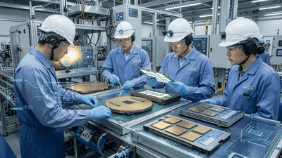
ASE comes from yet another direction. Traditionally, ASE has been the archetype of the outsourced semiconductor assembly and test provider: the company you go to once your wafers are finished and you need them turned into reliable packages, tested, and shipped at scale. ASE has decades of experience in everything from wire bonding and standard BGA packages to flip‑chip and system‑in‑package solutions.
In the advanced packaging era, ASE has decided not to sit on the sidelines. It has built up significant capabilities in:
- 2.5D and 3D packaging, including HBM integration.
- Fan‑out wafer‑level and panel‑level packaging.
- Multi‑chip modules and system‑in‑package designs that mix logic, memory, RF, and passives.
What makes ASE’s position unique is its role as a neutral integrator. Where TSMC and Intel combine foundry and packaging, ASE works with wafers and chiplets from many different sources. That enables:
- Mix‑and‑match integration. ASE can assemble packages that combine dies from different foundries, nodes, or even vendors, as long as interfaces and design rules line up.
- Design diversity. Customers can pursue heterogeneous integration strategies that aren’t locked into a single foundry’s ecosystem.
- Capacity relief. When CoWoS or other captive advanced lines are jammed, chipmakers and even foundries themselves may turn to ASE and other OSATs for overflow and complementary capacity.
ASE’s challenge, and its opportunity, is to scale these advanced services and match the yield and reliability expectations set by the integrated players. But its long history in packaging, broad customer base, and deep test expertise give it a strong foundation to build on.
Three Different Business Models, One Converging Goal
TSMC, Intel, and ASE are racing along the same track—advanced packaging and heterogeneous integration—but their business models point them in different directions:
- TSMC is the integrated, wafer‑centric turnkey provider: design in, wafers and advanced packages out, all under one umbrella.
- Intel is the architecture‑heavy foundry challenger, using packaging as a weapon to attract external customers and differentiate its own products.
- ASE is the flexible integrator, bridging multiple sources of silicon and offering packaging and test as a service to a wide range of customers.
Underneath those differences, the goal is remarkably similar: to become the go‑to platform for assembling heterogeneous systems in the AI and HPC era. Whether that means stacking chiplets, integrating HBM, or preparing for co‑packaged optics, advanced packaging is the gateway—and winning that gateway position means owning a lot of the value that used to be concentrated only in the wafer.
Technology Showdown: CoWoS, EMIB/Foveros, and OSAT Platforms
The race is not purely a business contest; it’s also a technology shootout. The three players emphasize different platforms:
TSMC’s CoWoS and 3DFabric
TSMC’s flagship for AI is CoWoS, a 2.5D approach that places big logic dies and multiple HBM stacks on a silicon interposer, which in turn sits on an organic substrate. Its strengths include:
- Very high bandwidth between logic and memory.
- Flexibility to support multiple HBM generations and channel counts.
- Proven viability at high volume for top‑tier AI accelerators.
Beyond CoWoS, TSMC’s SoIC and 3DFabric push into 3D stacking, offering potential for logic‑on‑logic and logic‑on‑cache configurations that could redefine high‑end CPUs and GPUs.
Intel’s EMIB and Foveros
Intel responds with its own combination:
- EMIB for high‑density horizontal interconnects between dies, embedded directly into the substrate where needed.
- Foveros for vertical stacking, combining compute tiles, cache, and other functions in a 3D configuration.
EMIB can be especially attractive when you want the benefits of 2.5D‑like integration without the cost and complexity of a full interposer. Foveros, meanwhile, enables tall stacks and creative floorplans that can reduce footprint and improve performance. Together, they give Intel a toolkit for both 2.5D and 3D heterogeneous integration in a way that is tightly connected to its foundry offerings.
ASE’s OSAT‑Style Platforms
ASE’s portfolio is broader and more customer‑driven. It may:
- Provide fan‑out and panel‑level solutions for mobile and automotive SoCs.
- Offer 2.5D and 3D packaging flows for HBM‑enabled accelerators.
- Develop custom SiP modules that mix logic, memory, RF, sensors, and passives in one package.
The key is flexibility: ASE often builds “platforms” around certain popular package types and then customizes them for specific customers. It’s less about owning a single branded technology like CoWoS or Foveros, and more about using a wide toolbox to serve many heterogeneous integration needs.
Capacity, Yield, and the AI Bottleneck
In the abstract, advanced packaging is about clever architectures. In the real world, it’s about whether you can ship millions of high‑value packages with acceptable yield and lead time. AI has turned capacity and yield into the main scorekeepers of this race.
TSMC enjoys a lead in both CoWoS capacity and yield, which is why so many AI products depend on it—and why its lines are so crowded. Intel is working to ramp its EMIB and Foveros lines to become a credible alternate source, attracting both internal and external designs. ASE, along with other OSATs, is scaling its advanced lines to take on more complex 2.5D/3D and HBM integrations, sometimes even acting as a relief valve when foundry‑run packaging is oversubscribed.
This capacity dynamic has a few interesting consequences:
- It forces chipmakers to think about packaging capacity as early as they think about wafer capacity.
- It encourages diversification; few customers want to depend on a single packaging provider for their entire AI roadmap.
- It creates opportunities for ASE and Intel when TSMC’s CoWoS lines are full, even if TSMC remains the technical leader.
In other words, the bottleneck is not just who has the best packaging technology, but who can deliver it at scale when the industry is hungry for AI performance.
What This Race Means for Heterogeneous Integration
From a system designer’s perspective, the three‑headed race brings both complexity and opportunity. On one hand, the landscape is more fragmented: different foundries and OSATs offer different packaging platforms, with different rules and capabilities. On the other hand, the competition drives innovation and gives designers more levers to pull:
- TSMC customers can lean into CoWoS and SoIC for massive GPU/AI packages and advanced 3D integration.
- Intel customers can explore EMIB/Foveros‑based chiplet architectures that may better align with their system goals and geographic preferences.
- Customers working with ASE can pursue multi‑foundry, multi‑vendor heterogeneous systems, knowing that a neutral OSAT can help bring the pieces together.
In all cases, advanced packaging and heterogeneous integration cease to be “back‑end” concerns and become central architectural decisions—choices that can make or break a product’s performance, cost, and time‑to‑market.
Looking Ahead: Collaboration, Not Just Competition
It’s tempting to view the advanced packaging race as a simple contest with a single winner, but reality is more nuanced. The market is large and growing, and different players may dominate different segments:
- TSMC leading in top‑end AI accelerator packaging and advanced 3D integrations tied to its logic nodes.
- Intel carving out a strong position in chiplet‑heavy designs and customers who value its geographic footprint and architectural offerings.
- ASE continuing to expand as the leading OSAT for heterogeneous integration across many markets, from mobile and consumer to automotive and networking.
There will also be plenty of collaboration. Foundries may outsource some packaging flows to OSATs to relieve bottlenecks. OSATs may work closely with both TSMC and Intel on jointly qualified flows. Customers may design systems explicitly to be portable across multiple packaging platforms.
What’s clear is that advanced packaging is no longer a support function. It’s where some of the most intense innovation and strategic maneuvering in semiconductors is happening. In that world, watching TSMC, Intel, and ASE is less about placing a bet on a single champion and more about understanding how their different approaches are collectively pulling the industry into a new era of heterogeneous, package‑centric computing.
The three‑headed race is just getting started—and for system designers, investors, and policy makers alike, it’s one of the most important races to follow. The winners won’t just define how chips are packaged; they’ll shape how the next generation of AI, HPC, and connected systems are built from the ground up—or more accurately, from the package up.
You May Like

Narrowing Spread Between NAND Spot and Contract Prices in 2026 – A Signal
By 2026, one of the most watched metrics in the NAND flash market has started to shift in a subtle but meaningful way: the spread between spot prices and long‑term contract prices is narrowing. For casual observers, this may look like just another incremental change in a notoriously volatile industry. For memory makers, module houses, device OEMs, and data center buyers, however, a tightening gap between spot and contract prices is a signal—a reflection of evolving supply–demand balance, risk perceptions, and strategic behavior on both sides of the market.

Price Divergence Trading Strategies Between NAND Flash and DRAM ETFs
NAND flash and DRAM sit at the core of AI storage and computing power. Both are memory, but they are not the same business. DRAM is main memory—fast, volatile, and central to high‑bandwidth workloads like AI training and inference. NAND is non‑volatile storage—slower than DRAM, but crucial to persistent data and large‑scale object storage. The cycles that drive their pricing and margins overlap, yet they often diverge. That divergence is where trading strategies between NAND and DRAM ETFs become interesting.

China’s HBM Localization Progress: The Catch-Up Pace of CXMT and XMC
China’s drive to localize advanced memory technologies has accelerated over the past several years. High-Bandwidth Memory (HBM) sits near the center of that strategy because it is integral to AI accelerators, high-performance computing (HPC) and other strategic compute platforms. Two domestic players—ChangXin Memory Technologies (CXMT) and XMC (Xianghui Memory, commonly referred to as XMC)—have become focal points in assessing how quickly China can close the gap with international incumbents on HBM die, stacking, and packaging.

Thermal Simulation Challenges and Solutions in 3DIC AI Chip Design
As AI workloads push chips to deliver ever higher compute density, designers are increasingly turning to three‑dimensional integration (3DIC) to stack dies vertically and pack more functionality into limited footprints. While 3DIC architectures unlock significant performance and bandwidth advantages, they also introduce complex thermal behaviors that are far harder to predict and manage than in traditional 2D layouts.

An Attempt at Compiling a Memory+Compute Fusion Thematic Index – A Dual-Track Framework
Most AI investors talk about “compute” as if it were the whole story: GPUs, accelerators, chips, cores. But every one of those cores needs somewhere to read from and write to. Memory and storage define how wide the data highway really is. In practice, AI performance is a fusion of compute and memory, not a solo act. So why do so many indices and ETFs separate them into different silos—one for semiconductors, one for memory, one for data centers—when the actual workloads keep blending them?
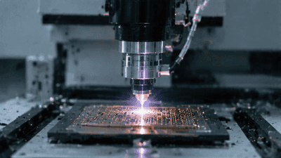
Surging Demand for Laser Drilling and Plasma Dicing Equipment in Advanced Packaging
Advanced packaging has become one of the semiconductor industry’s most important growth engines, and it is now pulling a surprising set of process tools into the spotlight. Among the most in-demand are laser drilling and plasma dicing equipment. These machines sit close to the heart of heterogeneous integration, fan-out packaging, wafer thinning, TSV formation, glass substrate processing, and other advanced flows where precision, yield, and throughput matter enormously. As packaging moves from a back-end afterthought to a strategic platform, the equipment used to shape, open, and separate materials has become just as important as the dies themselves.

D2D Interface Bandwidth and Latency Comparison in Chiplet Architectures
Chiplet architecture has turned the package into a real performance battleground. Once multiple dies are placed side by side or stacked within the same advanced package, the quality of the die-to-die, or D2D, interface becomes one of the most important determinants of system behavior. Bandwidth is no longer a nice-to-have metric, and latency is no longer a small implementation detail. Together, they shape whether a chiplet system feels nearly monolithic or frustratingly fragmented.

Stock Selection Logic and Alpha Validation of ESG-Themed Semi ETFs
Semiconductor themed ETFs are no longer just about growth and cycles. A growing subset now layers environmental, social, and governance (ESG) criteria on top of traditional sector exposure. These ESG semi ETFs promise two things at once: access to one of the market’s most powerful secular themes, and alignment with sustainability and governance standards. The pitch is appealing, but it raises two hard questions. First, how exactly are these stocks being selected? Second, does the ESG overlay help, hurt, or leave alpha unchanged?